
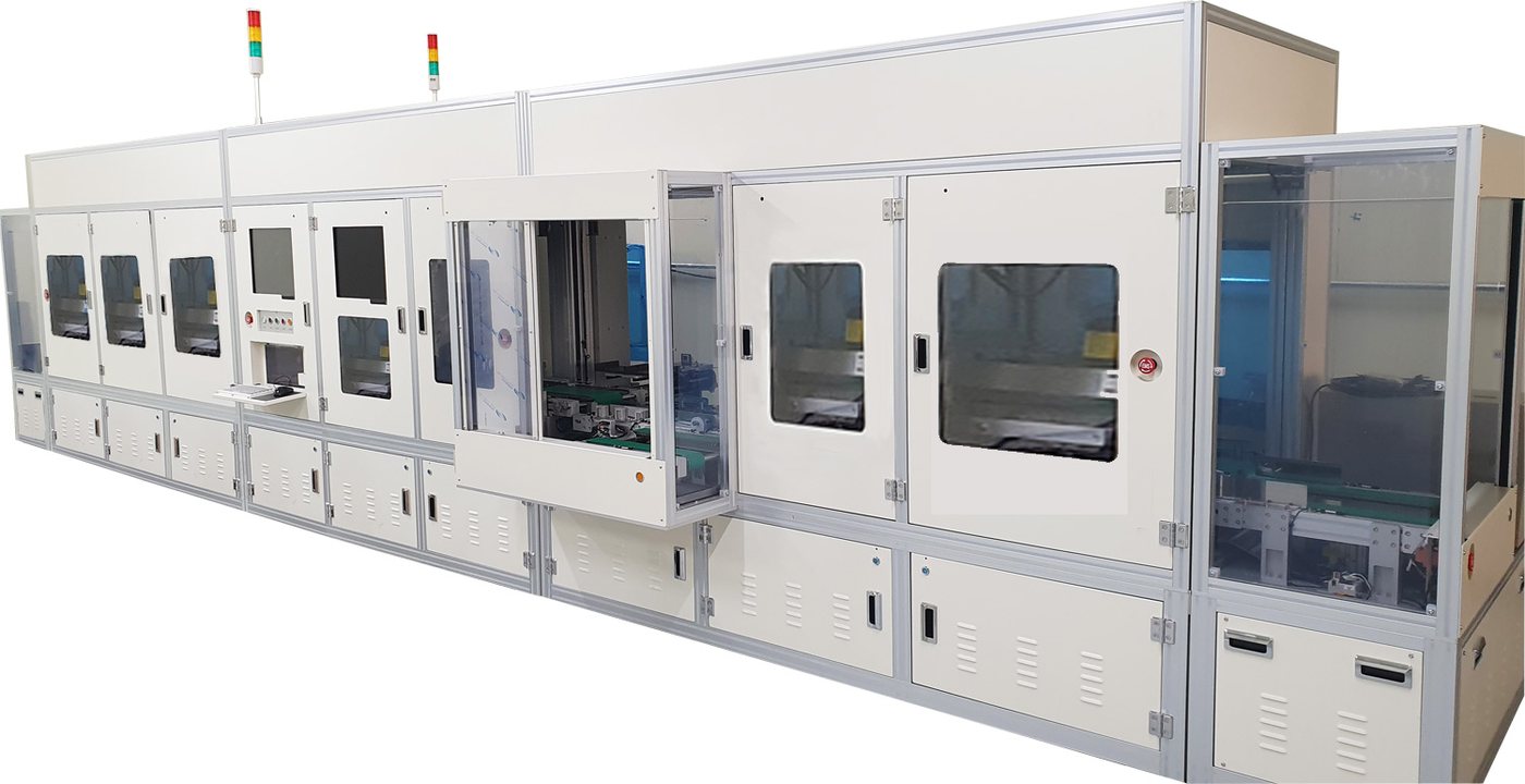
PKG Inspection System
System that inspects Marking, Mold Surface, Ball Land after Marking process for super thin type semiconductor package
Features
- Applicable to FCBGA Substrate
- Inspection on the front and back side surface of substrate
- Accuracy : 10um
- Mold : Chip out, Incomplete mold, Void hole, Bubble, Porosity, Crack Sticking, Scratch
- Marking : Illegible Mark, Double Mark, Incorrect orientation, Wrong Mark, Misplace Mark, No Mark
- Ball Land : Cu Exposure, Scratch, Contamination, Foreign Material, Sub Broken/Pressed
- Composition
- M/Z Loading, Transfer Rail, Top Vision Inspection, Btm Vision Inspection, M/Z Unloading